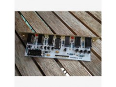
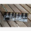
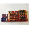
1.Shenzhen Jie Du State Technology Co., Ltd.(referred to as "Jieduo state technology"),was established in 2013-02-27, is Chinese earlier established PCB SMT factory phone company. Shenzhen Jie Du State Technology Co., Ltd.is Headquartered in Guangdong ProvinceGuangdong Province, it set up a subsidiary in Guangdong Provinceand Guangdong Province,Now there are about employees in the company, of whom are special PCB prototypete 2.Shenzhen Jie Du State Technology Co., Ltd. is specialized in 工业品,电子元器件,PCB电路板 since established in 2013-02-27 at 2013-02-27. So far,our company has established its branch companies in major cities throughout the country.Formed in Shenzhen,Futian district as the center, the radiation sales system and service network.Details:PCB Assembly Design in different stages need to set up different points in the layout phase can be used to carry out large grid layout of the device; For IC, non-positioning connectors and other large devices, you can use 50 ~ 100mil lattice precision layout, and for resistive capacitors and inductors and other passive small devices, can be used 25mil grid points for the layout. The accuracy of the grid is conducive to the alignment of the device and the appearance of the beautiful. PCB layout rules: 1, under normal circumstances, all components should be arranged on the same side of the circuit board, only the top components too dense, in order to some limited and small heat of the device, such as chip resistors, chip capacitors, paste Chip IC on the bottom. 2, in ensuring the electrical performance of the premise, the components should be placed on the grid and parallel to each other or arranged in order to be neat, beautiful, in general, does not allow the components overlap; components to be compact, the components in the entire layout should Uniform distribution, density consistent. 3, the different components on the circuit board adjacent to the minimum spacing between the drawings should be more than 1MM. 4, from the edge of the circuit board is generally not less than 2MM. The best shape of the circuit board is rectangular, aspect ratio of 3: 2 or 4: 3. circuit board ruler greater than 200MM by 150MM, should consider the circuit board can withstand Mechanical strength. Layout skills In the PCB layout design to analyze the circuit board unit, according to the function of the layout design, the circuit of all components layout, to meet the following principles: 1, according to the circuit of the process of arranging the location of the various functional circuit unit, so that the layout of the signal flow, and make the signal as much as possible to maintain the same direction. 2, to each functional unit of the core components as the center, around him to the layout. Components should be uniform, overall, compact arrangement on the PCB, to minimize and shorten the lead between the components and connections. 3, in the high frequency of the circuit, to consider the distribution of components between the parameters. General circuit should be arranged as far as possible in parallel components, so not only beautiful, but easy to install and easy to mass production. 3.Adhering to the "Customer Supreme Forge Ahead" management idea, Jieduo state technology insists on providing the best quality and service of PCB SMTx19b655en,PCB Assembly Manufacturer with the "customer first" principle. Wholeheartedly welcome your patronage! Official website address: www.pcbgogo.com