


Electronic packaging requires the substrate material to meet the high thermal conductivity, low dielectric constant, and the chip with the thermal expansion coefficient, good processing performance, high mechanical strength requirements. Due to the characteristics of the ceramic substrate coefficient, good heat conductivity, heat resistance, insulation, and chip matched thermal expansion in electronic packaging applications such as LED, CPV, and insulated gate bipolar transistor, laser diode package more widely.
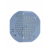
With the continuous development of LED lighting and sensor market and the expansion of scale, the demand for ceramic substrate has also been greatly improved. Especially the use of ceramic laser drilling technology prepared has high precision, vertical graphics package, can be realized through hole metallization, the holes can be large-scale production of single-sided and double-sided ceramic substrate etc., greatly improving the package of high power electronic devices integration.
Product features:
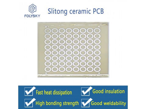
The ceramic circuit board has high accuracy and good electrical and thermal properties
2. ceramic circuit board with high bonding strength and good weldability, can realize blind through hole
3. ceramic circuit board technology is mature, environmental protection, pollution-free, cost is lower than traditional technology
4., a wide range of applications, single-sided and double-sided three-dimensional ceramic circuit boards can be produced
5. customized production, without mold opening, short production cycle
6., no organic ingredients, resistant to cosmic radiation, high reliability in aviation and space, long service life.
7. can carry out high-density assembly, line / pitch (L/S) resolution can reach 20 m, so as to realize the integration and miniaturization of equipment.
8. high frequency loss, it can be used in high frequency circuit.
9. copper sealing, high reliability.
10. 3D substrate and 3D routing.
1. ceramic circuit board appearance size is not limited
2., ceramic laser printing, three-dimensional routing
3. ceramic circuit board without mask, fast response
4. ceramic circuit board technology is mature, environmental protection, pollution-free
Product features:
1. the shape of the substrate is unlimited
2. laser printed 3D routing
3., no mask, fast response
4., mature technology, environmental protection, pollution-free
5. customized production, without mold opening, short production cycle
6.,no organic ingredients, resistant to cosmic radiation, high reliability in aviation ? ? and space, long service life.
7. can carry out high-density assembly, line / pitch (L/S) resolution can reach 20 m, ? ? so as to realize the integration and miniaturization of equipment.
8. high frequency loss, it