| Base Material |
FR-4,FR2.Taconic,Rogers, CEM-1 CEM-3,ceramic,crockery,Metal,Alumini |
| Copper Thickness |
1/2 oz min; 12 oz max |
| Board Thickness |
0.2mm-6mm(8mil-126mil) |
| Min. Hole Size |
0.1mm(4mil) |
| Min. Line Width |
0.075mm(3mil) |
| Min. Line Spacing |
0.1mm(4mil) |
| Surface Finishing |
HASL / HASL lead free, Chemical tin, Chemical Gold, Immersion Gold |
Payment & Shipping Terms:
| FOB Price: |
US $ 0.1-0.2/ Piece
Get Latest Price |
| Minimum Order Quantity: |
5 Piece/Pieces |
| Port: |
ShenZhen port |
| Packaging Details: |
1. at buyer's reqest; 2. inner,vaccum package; 3. outer, standard export carton |
| Delivery Time: |
PCB:8-10 days,PCBA:20-25 days |
| Payment Terms: |
L/C,D/A,D/P,T/T,Western Union,MoneyGram,paypal |
| Supply Ability: |
50000 Square Meter/Square Meters per Month |
Detailed Product Description
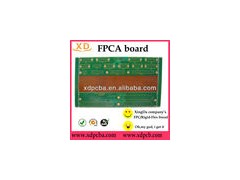
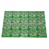
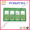
Flexible PCB With Carbon Ink Used For Keypad
1.Low cost flexible PCB,high quality,best service. 2.ISO14001:2000,ISO9001:2000/UL
FR4 1-38 Layer PCB;low price pcb manufacturer;Pcb Routing;Pcb Cutting Machine;Electronic pcb board;FR4 Double-sided PCB, Flexible PCB With Carbon Ink Used For Keypad , pcb for voltmeter , thin flexible pcb, Flexible PCB With Carbon Ink Used For Keypad

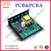
We can prvide a package of service:
· 1. PCB layout, PCB design;
· 2: Make high difficulty PCB(1 to 38 layers)
· 3: Provide all Electronic components;
· 4: PCB assembly;
· 5: Write programs for clients;
· 6: PCBA/finished product Test.
Specification for PCB Manufacture:
|
Item
|
Specification
|
|
Numbr of Layer
|
1-38Layers
|
|
Material
|
FR-4,FR2.Taconic,Rogers, CEM-1 CEM-3,ceramic , crockery
|
|
Metal-backed Laminate
|
|
Remarks
|
High Tg CCL Is Availabe(Tg>=170ºC)
|
|
Finish Board Thickness
|
0.2mm-6.00 mm(8mil-126mil)
|
|
Minimun Core Thickness
|
0.075mm(3mil)
|
|
Copper Thickness
|
1/2 oz min;12 oz max
|
|
Min.Trace Width & Line Spacing
|
0.075mm/0.1mm(3mil/4mil)
|
|
Min.Hole Diameter for CNC Driling
|
0.1mm(4mil)
|
|
Min.Hole Diameter for punching
|
0.9mm(35mil)
|
|
Biggest panel size
|
610mm*508mm
|
|
Hole Positon
|
+/-0.075mm(3mil) CNC Driling
|
|
Conductor Width(W)
|
+/-0.05mm(2mil)or
|
|
+/-20% of original artwork
|
|
Hole Diameter(H)
|
PTH L:+/-0.075mm(3mil)
|
|
Non-PTH L:+/-0.05mm(2mil)
|
|
Outline Tolerance
|
+/-0.125mm(5mil) CNC Routing
|
|
+/-0.15mm(6mil) by Punching
|
|
Warp & Twist
|
0.70%
|
|
Insulation Resistance
|
10Kohm-20Mohm
|
|
Conductivity
|
<50ohm
|
|
Test Voltage
|
10-300V
|
|
Panel Size
|
110×100mm(min)
|
|
660×600mm(max)
|
|
Layer-layer misregistration
|
4 layers:0.15mm(6mil)max
|
|
6 layers:0.25mm(10mil)max
|
|
Min.spacing between hole edge to circuity pqttern of an inner layer
|
0.25mm(10mil)
|
|
Min.spacing between board oulineto circuitry pattern of an inner layer
|
0.25mm(10mil)
|
|
Board thickness tolerance
|
4 layers:+/-0.13mm(5mil)
|
|
6 layers:+/-0.15mm(6mil)
|
|
Impedance Control
|
+/-10%
|
|
Different Impendance
|
+-/10%
|