| Place of Origin |
Guangdong, China (Mainland) |
| Brand Name |
Xing Da |
| Number of Layers |
1-38 |
| Base Material |
FR-4 , aluminium |
| Copper Thickness |
1/2 oz min;12 oz max |
| Board Thickness |
0.2mm-6.00 mm(8mil-126mil) |
| Min. Hole Size |
0.1mm(4mil) |
| Min. Line Width |
0.075mm(3mil) |
| Min. Line Spacing |
0.1mm(4mil) |
| Surface Finishing |
HASL / HASL lead free, OSP, Gold Finger Plating |
| Hole Position |
+/-0.075mm(3mil) CNC Drilling |
| Conductor Width(W) |
0.05mm(2mil)or;+/-20% of original artwork |
| Hole Diameter(H) |
PTH L:+/-0.075mm(3mil);Non-PTH L:+/-0.05mm(2mil) |
| Outline Tolerance |
0.125mm(5mil) CNC Routing;+/-0.15mm(6mil) by Punching |
| Warp & Twist |
0.70% |
| Insulation Resistance |
10Kohm-20Mohm |
| Conductivity |
<50ohm |
| Test Voltage |
10-300V |
Payment & Shipping Terms:
| FOB Price: |
US $ 0.2-10/ Piece
Get Latest Price |
| Minimum Order Quantity: |
1 Piece/Pieces |
| Port: |
Shenzhen/HK |
| Packaging Details: |
1. at buyer's request 2. inner, vacuum package 3. outer, standard export carton |
| Delivery Time: |
3-5 workdays |
| Payment Terms: |
L/C,D/A,D/P,T/T,Western Union |
| Supply Ability: |
50,000 Square Meter/Square Meters per Month |
Detailed Product Description
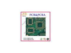
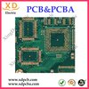
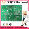
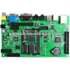
professional bga pcb
1.size:125*75mm
2.board thickness:FR-4 1.6mm
3.professional multi-layer bga pcb factory
4.Rohs
Welcome to XingDa Electric Technology Co., Ltd
Xindaxing Electric Technology Co., Ltd
We are professional manufacturer in various PCB and PCBA for many years .We can provide a reasonable price with high quality products.
XingDa who can provide a full set of service.such as below:
* 1. PCB layout, PCB design
* 2: Make high difficulty PCB (1 to 38 layers)
* 3: Provide all Electronic component
* 4: PCB assembly
* 5: Write programs for clients
* 6: PCBA/finished product Test. etc.
1. PCB Specification detail.
|
|
Item
|
Specification
|
|
|
1
|
Number of Layer
|
1-38Layers
|
|
|
2
|
Material
|
FR-4,FR2.Taconic,Rogers, CEM-1 CEM-3,ceramic , crockery Metal-backed Laminate
|
|
| |
|
3
|
Finish Board Thickness
|
0.2mm-6.00 mm(8mil-126mil)
|
|
|
4
|
Minimum Core Thickness
|
0.075mm(3mil)
|
|
|
5
|
Copper Thickness
|
1/2 oz min;12 oz max
|
|
|
6
|
Min. Trace Width & Line Spacing
|
0.075mm/0.1mm(3mil/4mil)
|
|
|
7
|
Min. Hole Diameter for CNC Drilling
|
0.1mm(4mil)
|
|
|
8
|
Min. Hole Diameter for punching
|
0.9mm(35mil)
|
|
|
9
|
Biggest panel size
|
610mm*508mm
|
|
|
10
|
Hole Position
|
+/-0.075mm(3mil) CNC Drilling
|
|
|
11
|
Conductor Width(W)
|
0.05mm(2mil)or;+/-20% of original artwork
|
|
|
12
|
Hole Diameter(H)
|
PTH L:+/-0.075mm(3mil);Non-PTH L:+/-0.05mm(2mil)
|
|
|
13
|
Outline Tolerance
|
0.125mm(5mil) CNC Routing;+/-0.15mm(6mil) by Punching
|
|
|
14
|
Warp & Twist
|
0.70%
|
|
|
15
|
Insulation Resistance
|
10Kohm-20Mohm
|
|
|
16
|
Conductivity
|
<50ohm
|
|
|
17
|
Test Voltage
|
10-300V
|
|
|
18
|
Panel Size
|
110×100mm(min);660×600mm(max)
|
|
|
19
|
Layer-layer misregistration
|
4 layers:0.15mm(6mil)max;6 layers:0.25mm(10mil)max
|
|
|
20
|
Min. spacing between hole edge to circuity pattern of an inner layer
|
0.25mm(10mil)
|
|
|
21
|
Min. spacing between board outline to circuitry pattern of an inner layer
|
0.25mm(10mil)
|
|
|
22
|
Board thickness tolerance
|
4 layers:+/-0.13mm(5mil);6 layers:+/-0.15mm(6mil)
|
|
|
23
|
Impedance Control
|
+/-10%
|
|
|
24
|
Different Impedance
|
+-/10%
|
|
2.Details for PCB Assembly
Technical
1).Professional surface mounting and through hole soldering technology;
2).Various sizes ,like 1206,0805,0603 components SMT technology;
3).ICT(In Circuit Test),FCT(Functional Circuit Test) technology;
4).Nitrogen gas reflow soldering technology for SMT;
5).High standard SMT& Solder Assembly line;
6).High density interconnected board placement technology capacity.
Quote requirement
1).The detailed files(Gerber files ,specification and BOM);
2).Clear pictures of PCBA or samples for us;
3).PCBA Test method.