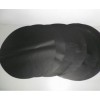
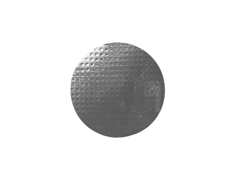
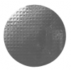


Anti-Static Wafer Pad PS is an anti-static packaging material specially designed for semiconductor wafers, which is mainly used to prevent damage to wafers caused by static electricity accumulation and discharge during storage, transportation and processing.
Material and Properties:
Anti-Static Wafer Pad PS is mainly composed of anti-static polystyrene (PS) material, which undergoes special processing to enhance its electrostatic dissipation properties. Its surface resistivity is typically maintained between 10^5 and 10^9 ohms/square to effectively prevent the buildup of static electricity.
The Antistatic PS material itself exhibits strong mechanical characteristics such as moderate hardness, impact resistance, light weight, and ease of molding and processing, making it well-suited for the precise packaging needs of semiconductor wafers.